


The transfer molding method, for which we take advantage of our extensive track record and reliability, and the compression molding method, with which we will respond to future demand for panels and slimmer dimensions.
Our Commitment to Technologies
Plastic Molding Technologies/Transfer Molding and Compression Molding
In semiconductor plastic encapsulation technology, molding can be roughly divided into transfer and compression methods. Since establishing industry standards by developing the world’s first fully automated semiconductor plastic encapsulation equipment with multi plunger, TOWA has been the leading company in the semiconductor molding market. In addition to transfer systems boasting many years of experience, we propose a molding process that stays ahead of the needs of the market with the newly developed compression method as state-of-the-art encapsulation technology.
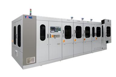
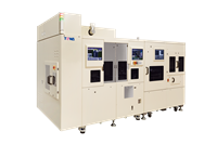
Molding using the transfer method and the compression method
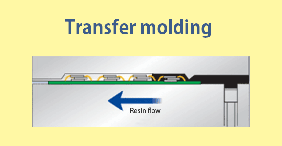
Transfer Method
Transfer molding is a conventional method of plastic encapsulation of electronic components, such as semiconductors, with which the cavity is filled with melted resin by using a plunger.
The multi plunger system that supplies resin from multiple holes when injecting resin into the cavity is a molding method that we developed in the early years, in addition to a drastic improvement in resin use efficiency and significant improvement in molding quality, it made it possible to greatly shorten the resin molding cycle, being highly valued all over the world.
Due to the reliability and achievements of our transfer molding method which became the de facto standard, it has been adopted for a large number of products to date and by making use of this extensive accumulated know-how, we provide optimal solutions for our customers.
Molding using the transfer method
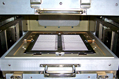
Molding using the compression method
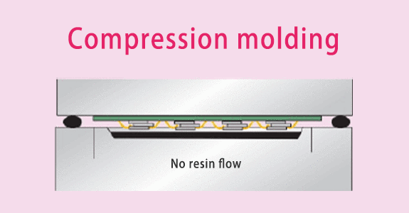
Compression Method
As demand for semiconductors is increasing in areas such as Internet of Things (IoT), self-driving cars, and expansion of data centers due to increase in data volume, devices such as tablets and smartphones are also diversifying.
Semiconductor packaging technology is also required to be thinner and more highly integrated. Wafer level package, which is molded omitting the substrate for achieving miniaturization and ultra-thinning, and a molding process that realizes high productivity and cost reduction are also requested. For responding to market needs ahead of others, we have developed a new molding technology based on the compression method.
Material cost reduction with 100% resin efficiency
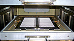
With the compression method, liquid or granular resin is put directly into the cavity and then melted before the workpiece is immersed in it for resin molding. This method makes it unnecessary to use a gate or a runner, which are used for the transfer method, and makes the efficiency in the use of resin almost 100%. The compression method contributes greatly to customer’s cost reduction and reduces the amount of waste, which makes it a more environmentally friendly molding technology than ever before.
No resin flow allowing thinner wires
With molding using the compression method, there is virtually no resin flow, which enables the impact on chips and wires to be minimized. It improves the molding quality of package products and permits the use of thinner wires, leading to the reduction of material costs.
Applicable to large size panels and wafers
For reducing the cost of semiconductor packages, lead frames and substrates sizes are becoming larger, requiring semiconductor manufacturing equipment that is compatible with them.
By using our compression technology, it’s possible to mold ultra large panels and offer solutions for industry cost reduction needs ahead of the market.
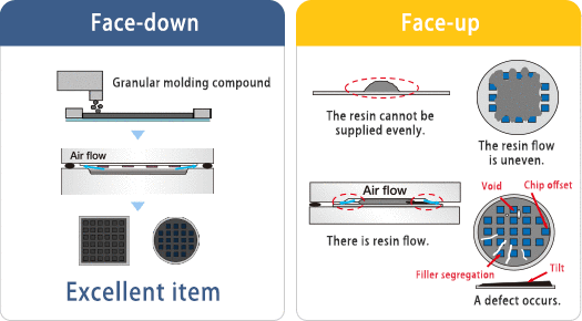
Face down method adopted
Due to thinner semiconductor packages, it is necessary to evenly and uniformly supply resin to panels and wafers with large mold area. By adopting the face down method, we have realized uniform and extremely thin molding even for large mold areas. And compared to the face up method, its superiority is recognized with less warpage generated during molding.
Reduced manufacturing process and cleaning-less
This method reduces the time taken for the overall manufacturing process because it does not require the processes after molding such as backgrinding and chemical mechanical polishing (CMP).
In addition, it uses a mold release film, which makes it unnecessary to clean the mold.
Our molding technology based on the compression method also reduces the pressure applied to the workpiece, enabling the molding of products made from low-K materials to be optimized.
Products such as 3D NAND flash memory, application processors, fingerprint sensors, power devices have been showing growth, and the compression method adapted to those devices has been high valued in the global market as an equipment with stable quality and productivity.
Benefits of TOWA’s face-down method
| Face-down | Face-up | |
|---|---|---|
| Resin flowability | ◯ | ✕ |
| Chip offset | ◯ | △ |
| Degree of Vacuum | ◯ | △ |
| SIP product | ◯ | ✕ |
| Filler segregation (a cause of warpage) | ◯ | △ |
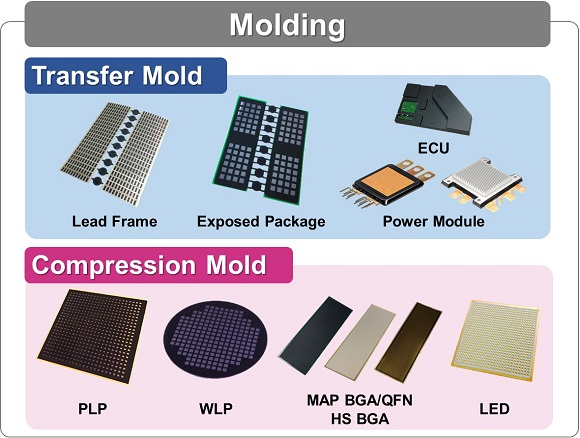
Product List
-
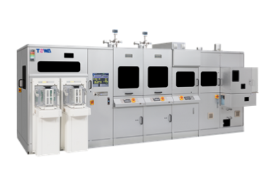
TOWA is a leading company in the semiconductor molding equipment market. We offer equipment using our proven transfer molding method, and high quality / flow free compression molding method.
-

With our expertise in the field of singulation, high speed handling and image analysis technology, we offer high quality singulation equipment.
-
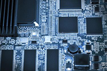
As the leading company in resin sealing technologies for semiconductors and other electronic components, we at TOWA Corporation have supplied a number of ultra-precision molds to the market. These products have been highly acclaimed by customers.
-
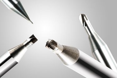
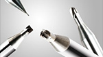
Developed by utilizing technologies cultivated through the manufacture of ultra-precision molds, End mills and Drills from TOWA boast high precision, superior abrasion resistance, and a long life-span.