


We work on the research and development of new materials, resin molding technologies, and microfabrication to further improve the level of the mold-manufacturing and resin-molding technologies that we have developed over many years and to create innovative technology. Achievements made through these research and development efforts are applied not only to the semiconductor field but also to other fields such as optics, healthcare, biochemistry.
Our Commitment to Technologies
Research & Development
Coating Technology
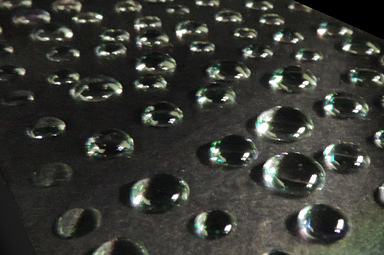
Bancera coating, which is our proprietary coating technology, is a coating technology that greatly improves the durability, releasability and antifouling properties of molds as compared with conventional coatings. It has been used not only for mold chases but also in a wide range of fields including pharmaceutica tableting machines, machine sliding parts of equipment, surface treatment to glass and the like.
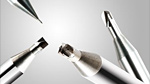
Ultra-Precision/Microfabrication Technology
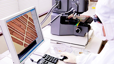
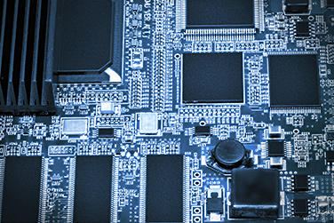
In order to make products smaller with higher performance, ultra precision micofabrication technology to minaturize constituent parts with high precision is necessary. At TOWA, we undertake research and development from a wide range of perspectives related to ultra-precision micro-fabrication, including the environment, devices, equipment, measurement, evaluation, tools, materials, and processing methods, it is compatible with various processing materials such as metal, resin and ceramics.
EF (Ultra-Precision Electroforming) Process Technology
EF (ultra-precision electroforming) process technology is effective for the mass production of molds that require complicated shapes and high precision. Using the same electrochemical reaction used in electroplating, EF process technology enables ultra-precision molds to be duplicated and produced within around 24 hours, while it takes 700 hours using the machining process. This greatly improves productivity and reduces cost.
Mold Design Technologies
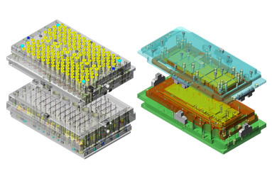
We design molds using a system where the processes from the creation of product drawings, layout, and the arrangement of parts to the creation of data for processing are automated based on 3D CAD data. To ensure optimal designs, we also examine the molds before producing them through CAE analysis using 3D data.
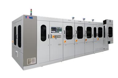
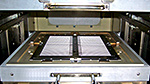
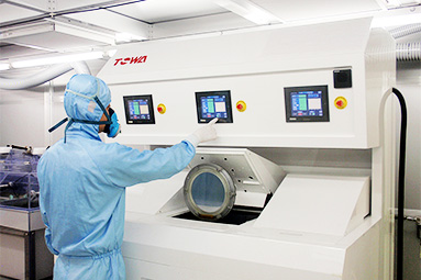
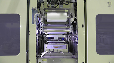
Plastic Molding Technologies/Transfer Molding and Compression Molding
In semiconductor plastic encapsulation technology, molding can be roughly divided into transfer and compression methods. Since establishing industry standards by developing the world’s first fully automated semiconductor plastic encapsulation equipment with multi plunger, TOWA has been the leading company in the semiconductor molding market. In addition to transfer systems boasting many years of experience, we propose a molding process that stays ahead of the needs of the market with the newly developed compression method as state-of-the-art encapsulation technology.
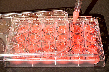
Fine Plastics

Plastics are essential materials in many industrial fields. Above all, engineering plastics with superior properties are used in telecommunications, information appliances, healthcare, optics, and other fields. Since our founding, we have maintained a consistent approach to the design, production, molding, and assembly of injection molds for engineering plastics. As a result, we provide high-quality molded products that are highly valued in the market.
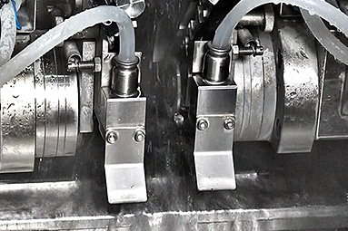
Press Design Technologies
We have been developing, manufacturing and selling semiconductor manufacturing equipment for many years. By taking advantage of our extensive track record, we design press modules in a manner that optimizes the shape of every single component part.
Automation Design Technologies
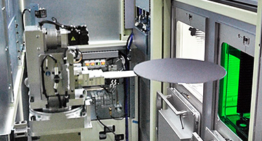
In the automation design of semiconductor manufacturing equipments, by handling materials and products with high speed and high precision, productivity and quality are improved. Our proprietary design automation technologies are used to better meet customers’ demands for quality and delivery of replacement parts for each product type.
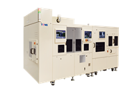
Singulation Technology
Singulation, one of core technologies in the post-process of semiconductor manufacturing, is a technology we are working on since the 1990s. We combine high-speed handling technology and image analysis technology with cutting technology that we have cultivated over many years, and we are offering high-quality singulation equipments.
Product Case
-

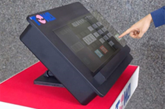
Introduce our manfufacturing technology used for finger print sensors.
-
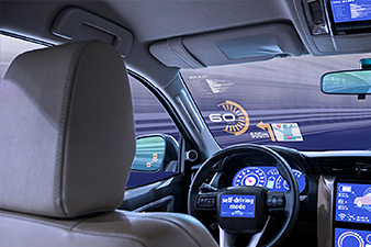
Introduce ultra precision element technologies that support the manufacturing of high quality and high precision optical parts used in head up displays.
-

Introduces our molding technologies andequipment, which improves the reliability of ECUs and various automotive electronic devices.
-
Introducing the floating image lens and various application examples based on our ultra-precision mold processing technology, EF technology, and injection molding technology.