


TOWA’s molding technology is used to manufacture fingerprint sensors, which smaller and thinner dimensions are being demanded.
Product Case

Finger Print Sensors
TOWA’s products and technology is used in various scenes of our everyday lives. Here we will introduce our manfufacturing technology used for finger print sensors.

- Resin sealing technologies that support the manufacture of finger print sensors
- Capable of handling a wide range of semiconductor manufacturing, from MAP molding to highly difficult MUF molding
- We enable the further downsizing and slimmer dimensions of finger print sensors.
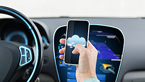
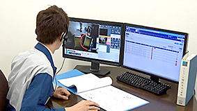
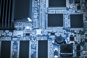
Finger print sensors used in various scenes of our everday lives
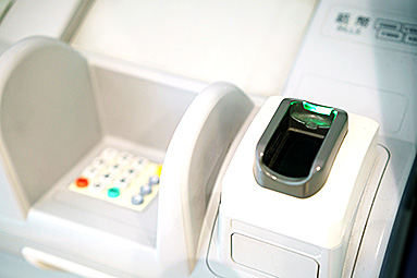
Finger print sensors that is widely used, including for bank ATMs
IC cards and password authentication is handy, but you may lose your card or forget your password. Someone other than yourself may be falsely authenticated by ID card theft or leakage of your password. To avoid such dangers, biometric authentication is widely used.
Among biometric authentication, fingerprint recognition is widely used in a variety of settings — such as access control, logins for PCs and systems, mobile phones and smartphones, and automatic teller machines (ATM) of banks — because it is easy to apply. The sensors used for this fingerprint recognition are required to be small and slim.
For mounting components on fingerprint sensors, a method called ball grid array (BGA) is widley used. BGA allows multiple terminals to be mounted and also a smaller mounting area because the leads do not protrude to the outside. It is therefore an appropriate manucturing method for fingerprint sensors, which are required to be compact in size.
Meanwhile, with regard to the slimmer dimensions required of fingerprint sensors, there is a shift from conventional wire bonding to the flip chip. A sealing technology called mold under fill (MUF) is used. MUF makes it possible to reduce package assembly cost and manufacturing hours as well as a thinner size.
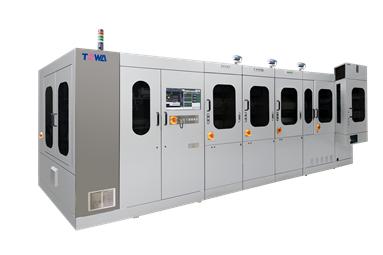
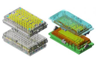
With many years of experience in transfer molding, our YPM series is widely applicable to manufacture MAP BGA, which is a high productive form of BGA packages, to difficult MUF applications and also finger print sensor applications.
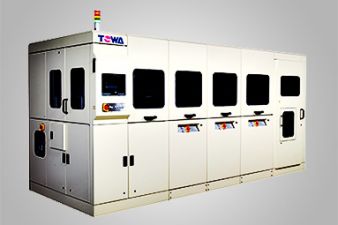
As fnger print sensors for smartphones require a thin platform, our compression molding equipment PMC, which can reduce the total thickness of the mold thickness from the top of the die, has been widely adpoted.
Applicable for WLCSP to support further miniaturization and thinner sensor
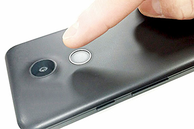
Fingerprint recognition system of a smartphone
In the future, it is expected that further miniaturization and thinning will be required by increasing the number of devices and usage scenes equipped with fingerprint sensors. The packaging method for fingerprint sensor will be shifted from BGA to WLCSP (Wafer Level Chip Scale Package).
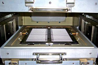
Our CPM series is a compression molding system compatible with wafer level molding, and it’s also applicable for the manufacture of FOWLP (Fan Out Wafer Level Package) in addition to WLCSP also called FIWLP (Fan In Wafer Level Package). With our CPM series which has thinning technology and high-accurate control technology, it is possible to further reduce the size and thickness of the fingerprint sensor.
Related Technologies Owned by TOWA
Related Products
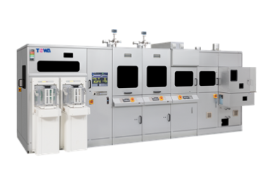
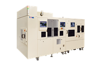
CPM-Series
The CPM-series molding equipment is capable of molding wafers and panels, which are growing larger, by utilizing the compression method.

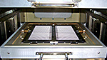
PMC-Series
PMC is a series of equipment that enables high-quality molding by utilizing the compression method. Cumulative sales of these pieces of equipment have exceeded 400 units.
YPM-Series
The YPM-series molding equipment utilizes our world-leading transfer method.