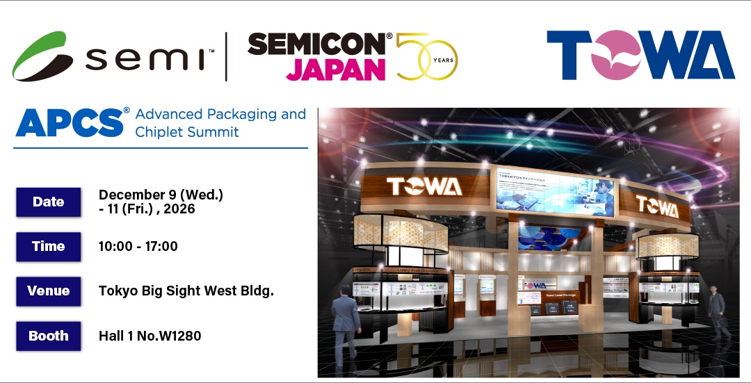

|
PICK UP |
Advanced Package |
PICK UP
Advanced Package
|
WLP/PLP Process |
|||
|
|
As advanced packaging technologies continue to evolve, driven by the diversification of memory integration and increasing package sizes, molding technology is becoming increasingly important. |
||
|
Laser Singulation Technology |
||||
|
High-speed laser dicing enables the processing of irregular shapes, fine-pitch features, and thick packages. Non-contact processing without grinding wheels helps reduce water consumption and the use of consumables, contributing to high quality and productivity. |
|
|||
|
MOLDING TOWA supports molding for a wide range of sizes, from wafers for advanced packaging to ultra-large panels measuring 700 mm × 700 mm. We offer molding solutions to meet diverse needs, including higher-density and 3D memory integration, increasing package sizes, automotive power semiconductors, and substrate-related applications. |
SINGULATION Laser and blade cutting technologies enable high-precision cutting of various semiconductor packages and mounting substrates. TOWA offers solutions to meet diversifying processing needs, including cutting of irregular shapes and thick packages, singulation of large panels, and warpage correction. |
|
LASER TOWA Laser Front Co., Ltd. introduces laser-based processing technologies such as wafer marking, cutting, trimming, and welding. |
THERMAL NANOIMPRINT TOWA is working toward the practical application of thermal nanoimprint technology by applying technologies developed through its semiconductor molding equipment business. The technology utilizes high-precision pressing and thermal pattern transfer using large-scale presses, along with vacuum molding technology. |
|||
|
SERVICE TOWATEC Co., Ltd. introduces a multi-faceted support system that sustains equipment lifecycles, including used equipment sales and purchase, equipment refurbishment, and scheduled maintenance. |
HAPPY HOUR TOWA will also be participating in Happy Hour! |
WLP/PLP Process
Total Solution
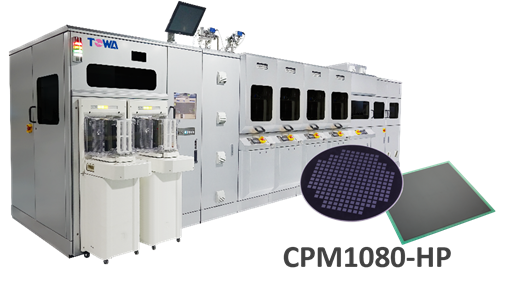
As advanced packaging technologies continue to evolve, driven by the diversification of memory integration and increasing package sizes, molding technology is becoming increasingly important.
With its proprietary compression molding technology, TOWA supports a wide range of sizes, from wafers to ultra-large panels, to meet diversifying market needs.
Furthermore, TOWA offers equipment covering processes from molding to singulation, providing comprehensive support for WLP/PLP manufacturing processes.
Laser Singulation Technology
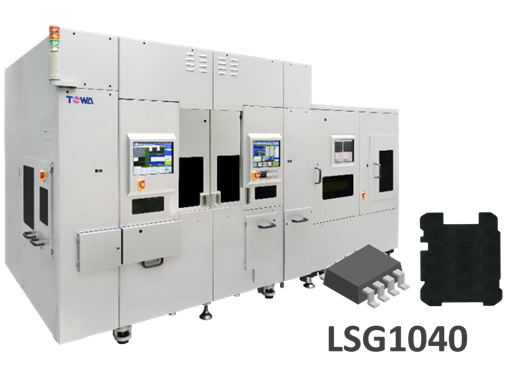
High-speed laser dicing enables the processing of irregular shapes, fine-pitch features, and thick packages. Non-contact processing without grinding wheels helps reduce water consumption and the use of consumables, contributing to high quality and productivity.
Furthermore, TOWA is advancing the development of its “4in1” technology, which aims to integrate multiple processing functions, including marking, into a single machine to meet customer needs.
MOLDING
TOWA supports molding for a wide range of sizes, from wafers for advanced packaging to ultra-large panels measuring 700 mm × 700 mm. We offer molding solutions to meet diverse needs, including higher-density and 3D memory integration, increasing package sizes, automotive power semiconductors, and substrate-related applications.
SINGULATION
Laser and blade cutting technologies enable high-precision cutting of various semiconductor packages and mounting substrates. TOWA offers solutions to meet diversifying processing needs, including cutting of irregular shapes and thick packages, singulation of large panels, and warpage correction.
LASER
TOWA Laser Front Co., Ltd. introduces laser-based processing technologies such as wafer marking, cutting, trimming, and welding.
THERMAL NANOIMPRINT
TOWA is working toward the practical application of thermal nanoimprint technology by applying technologies developed through its semiconductor molding equipment business. The technology utilizes high-precision pressing and thermal pattern transfer using large-scale presses, along with vacuum molding technology.
Compared with UV-based methods, it does not require light source equipment, helping reduce equipment and operating costs. TOWA aims to provide comprehensive support, from fine-pattern mold fabrication to contract molding services and equipment sales.
SERVICE
TOWATEC Co., Ltd. introduces a multi-faceted support system that sustains equipment lifecycles, including used equipment sales and purchase, equipment refurbishment, and scheduled maintenance.
HAPPY HOUR
December 10 (Thu), 16:00–17:00
TOWA will also be participating in Happy Hour!
We look forward to welcoming you with a selection of beverages at our booth.