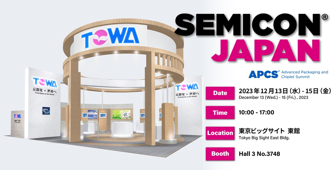
We are pleased to inform you that we will set up a booth at “SEMICON JAPAN 2023” .
We will introduce our molding technologies for a variety of packages,
including semiconductors for AI at the core of future technological innovation,
and the trending automotive semiconductors.
We also want to introduce our support system for customers around the world.
|
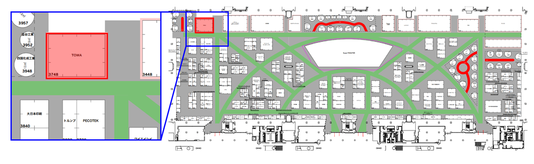
Date Time Location Booth Admission Fee |
December 13 (Wed.) to 15 (Fri.), 2023 10:00-17:00 Tokyo Big Sight East Bldg. Hall 3 No.3748 |
||
|
Date |
December 13 (Wed.) to 15 (Fri.), 2023 |
|
|
Time |
10:00-17:00 |
|
|
Location |
Tokyo Big Sight East Bldg. |
|
|
Booth |
Hall 3 No.3748 |
|
|
Admission Fee |
||
 |
Molding Technology for AI
Introduction of total solution including compression molding that contributes to WLP/PLP processes for 2.5D/3D/Chiplet and other cutting-edge semiconductors that are the focus of attention in generation AI. |
||
 |
Molding Technology for Mobile
Proposal of low-pressure molding technology + narrow GAP resin filling technology for devices such as RF modules and memory. In addition, we introduce molding technology for high heat dissipating materials and double-sided molding technology for multifunctionalities. |
||
 |
Molding Technology for Automotive
Proposal of exposed heat sink molding technology for power semiconductors. For automotive devices such as ECUs, we will introduce molding technologies that contribute to improve reliability and package miniaturization. |
||
 |
Singulation Technology
Introduction of individual piece cutting technology for products of various sizes. We also propose labor-saving equipment for automation. Introducing singulation technology and in-house blades that enable high-precision cutting of mounted products. |
||
 |
Laser Technology
TOWA LASERFRONT CORPORATION introduces wafer marking, cutting, trimming, and welding technologies with laser. |
||
 |
Laboratory and Manufacturing Support System
Proposal of laboratory activities to support prototype evaluation and process development for advanced packaging. Introduction of our consistent and reliable support system from customer inquiry and prototype evaluation to mass production. |
||
 |
Molding Technology for AI
Introduction of total solution including compression molding that contributes to WLP/PLP processes for 2.5D/3D/Chiplet and other cutting-edge semiconductors that are the focus of attention in generation AI. |
||
 |
Molding Technology for Mobile
Proposal of low-pressure molding technology + narrow GAP resin filling technology for devices such as RF modules and memory. In addition, we introduce molding technology for high heat dissipating materials and double-sided molding technology for multifunctionalities. |
||
 |
Molding Technology for Automotive
Proposal of exposed heat sink molding technology for power semiconductors. For automotive devices such as ECUs, we will introduce molding technologies that contribute to improve reliability and package miniaturization. |
||
 |
Singulation Technology
Introduction of individual piece cutting technology for products of various sizes. We also propose labor-saving equipment for automation. Introducing singulation technology and in-house blades that enable high-precision cutting of mounted products. |
||
 |
Laser Technology
TOWA LASERFRONT CORPORATION introduces wafer marking, cutting, trimming, and welding technologies with laser. |
||
 |
Laboratory and Manufacturing Support System
Proposal of laboratory activities to support prototype evaluation and process development for advanced packaging. Introduction of our consistent and reliable support system from customer inquiry and prototype evaluation to mass production. |
||
|
Tokyo Big Sight East Bldg. Hall 3 No.3748
|